
The contest has moved to rack scale
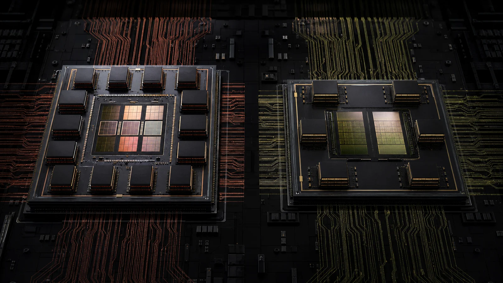
On July 23, 2026, AMD replaced the preliminary MI455X figures with a complete product brief. The CDNA 5 GPU has 432 GB of HBM High Bandwidth Memory. Stacked DRAM integrated into the accelerator package through a very wide interface. It provides several TB/s, although the exact packaging topology depends on the product. at 23.3 TB/s, 40.3 peak PFLOPS in OCP MXFP4 Microscaling FP4. A block format in which 32 FP4 values share one scale factor. That shared scale is what makes 4-bit storage usable without collapsing accuracy. NVIDIA's NVFP4 variant uses finer 16-value blocks. , and a 3.6 TB/s UALoE scale-up link. Its package combines eight compute XCDs, two I/O dies and two Fabric and Cache Dies carrying a 192-channel HBM4 interface and 192 MB of global L2 cache. Two days earlier, NVIDIA had detailed Rubin: 288 GB of HBM4 at 22 TB/s, 50 PFLOPS of NVFP4 inference, two compute dies joined through NV-HBI, and NVLink NVIDIA's proprietary GPU-to-GPU interconnect. NVLink 5 (Blackwell) reaches 1.8 TB/s bidirectional per GPU; NVLink 6 (Rubin) doubles that to 3.6 TB/s. With NVSwitch, it accelerates GPU-to-GPU transfers and collectives; memory remains physically distributed, and remote access does not have the cost of local HBM. at 3.6 TB/s.
Read too quickly, the comparison already looks settled. AMD places another 144 GB around every GPU and moves 1.3 TB more per second out of HBM. NVIDIA answers with a higher advertised 4-bit compute rate and a vertically integrated NVLink stack. That reading misses the mechanism that decides a distributed workload: a byte read from local HBM does not take the same path as an activation waiting on a neighboring GPU.
The useful question is not which data sheet contains the largest number. It is this: when does AMD’s extra capacity remove a communication step, and what happens once it can no longer remove it?
One GPU: 50% more capacity, 6% more bandwidth
| Characteristic | AMD MI455X | NVIDIA Rubin | Reading |
|---|---|---|---|
| Architecture | CDNA 5, 8 XCD + 2 IOD + 2 FCD | 2 compute dies linked by NV-HBI | Two multi-die packages |
| Transistors | 320 billion | 336 billion | Does not predict throughput |
| Memory | 432 GB HBM4, 12 stacks | 288 GB HBM4 | +50% for AMD |
| HBM bandwidth | 23.3 TB/s | 22 TB/s | +5.9% for AMD |
| Published 4-bit compute | 40.3 PFLOPS OCP MXFP4 | 50 PFLOPS NVFP4 inference; 35 training | Different formats and modes |
| Scale-up per GPU | 3.6 TB/s UALoE, bidirectional | 3.6 TB/s NVLink 6 | Equal published peak |
| Announced availability | Helios design, shipments H2 2026 | Rubin in production, systems H2 2026 | Vendor timelines |
Capacity is the most robust number in the table. It does not depend on a kernel or a vendor’s choice of arithmetic format. The MI455X physically contains 432 GB; Rubin contains 288 GB. The ratio is exactly 1.5. Memory bandwidth is also reasonably comparable because both vendors publish a package-level peak for HBM4. AMD’s 23.3 TB/s exceeds NVIDIA’s 22 TB/s by 5.9%, a real paper advantage, but a much smaller one than the capacity gap.
That contrast matters during decode The autoregressive generation phase of an LLM: one token is produced at a time while rereading weights and the relevant context state. At low batch sizes, that traffic can make decode memory-bandwidth-bound. Its share of total cost still depends on input and output lengths, batching and cache reuse. . Autoregressive generation rereads the weights and the KV cache The stored key and value vectors an LLM has already computed for every token it has processed. It avoids recomputing attention over the whole history, at the cost of a memory footprint that grows with the context length. for every token. Another 50% of capacity can keep more weights, context or concurrent requests on the same GPU. Another 5.9% of bandwidth promises, at the theoretical ceiling, only a gain of the same order on a workload that is strictly memory-bound. Capacity can change the number of GPUs required; bandwidth changes the time needed for one local read.
What 432 GB can actually avoid
A capacity boundary can be reasoned about before any benchmark. With 8-bit weights, a model with N billion parameters needs at least N GB for those weights. At 4 bits, that floor becomes N / 2 GB. These figures exclude scale factors, quantization metadata, runtime buffers and the KV cache. They describe a physical minimum, not a deployable configuration.
On that basis, 288 GB can hold at most 288 billion parameters at 8 bits, against 432 billion on MI455X. At 4 bits, the raw ceilings become 576 and 864 billion parameters. Both systems need headroom for the rest of the stack, so the useful boundary sits lower, but the relative gap does not change.
Consider a model whose active working set, meaning weights, cache and buffers, occupies 350 GB. It fits in one MI455X HBM pool. On Rubin, the operator must either lower precision, offload part of the state or distribute the model across at least two GPUs. The first option can change quality, the second adds a slower memory tier, and the third introduces an inter-GPU synchronization at every split layer.
Removing that hop is why capacity can matter more than PFLOPS. It lowers the degree of tensor parallelism Splitting one neural-network layer across several accelerators. Each GPU computes a partial output, then a collective operation merges the fragments before the next layer. The wider the split, the more interconnect latency and bandwidth contribute to the time per token. , and therefore the number of fragments that must wait for one another after each matrix multiplication. It does not guarantee that a model which fits on one GPU should remain there. A strict TPOT target may still require several GPUs to provide enough compute or bandwidth. The capacity advantage therefore tends to reduce the degree of sharding and free room for KV cache and concurrency, rather than eliminate every communication step.
A back-of-the-envelope calculation makes that margin more concrete. For a hypothetical model with 80 layers, 8 KV heads of dimension 128, and an FP8 cache, the keys and values require 2 × 80 × 8 × 128, or 163,840 bytes per token. The 144 GB gap then represents about 880,000 cached tokens across active sequences. This is an estimate under explicit assumptions, before memory alignment, fragmentation, buffers and metadata. A different model can produce a very different result.
The result is not “50% more memory means 50% more tokens.” It depends on the working set and service target. Below 288 GB, both GPUs can avoid a capacity-driven split. Between 288 and 432 GB, only AMD can avoid it. Above 432 GB, both enter a distributed regime.
Once the model spills, the interconnect becomes memory
Tensor parallelism splits a matrix across several GPUs. Each GPU reads its weight shard from local HBM, computes a partial output, then joins an all-reduce or all-gather to rebuild the activations required by the next layer. That rendezvous returns dozens of times per token. The fastest GPU cannot start the next layer until the expected data arrives.
MoE models add a different traffic pattern. Expert parallelism routes token activations to the GPUs hosting the selected experts, then returns them through an all-to-all. More HBM can keep more experts local or allow replication, but it does not remove routing while active experts remain distributed. For these models, small-message latency, all-to-all throughput and congestion control matter alongside the tensor-parallel all-reduce.
The transport hierarchy then becomes visible, but its conventions must be aligned. MI455X’s 23.3 TB/s and Rubin’s 22 TB/s are package HBM bandwidth figures. The 3.6 TB/s scale-up figure instead sums bidirectional link capacity. Dividing them therefore compares two data-sheet values that measure neither the same path nor the same operation; the quotient is not a performance multiplier. If bidirectional capacity is split symmetrically, the theoretical one-way envelope is 1.8 TB/s, but useful collective throughput still depends on message size, topology, parallel links and software. The robust conclusion is narrower: a byte retained in local HBM does not traverse the scale-up fabric.
The title can now receive its first answer. Memory beats NVLink only when it lets the system avoid using NVLink. Once both platforms shard a model across multiple GPUs, AMD’s capacity can still reduce the number of shards, but it no longer replaces the quality of the scale-up fabric.
UALoE matches NVLink on advertised bandwidth
AMD does not enter this generation with the same interconnect used by MI355X. Helios connects 72 MI455X GPUs through UALink Ultra Accelerator Link. An open scale-up communication standard for accelerators. It exposes reads, writes and atomic operations across a distributed address space, with coherency managed in software. AMD carries it over Ethernet in Helios under the name UALoE. over Ethernet, or UALoE. The UALink protocol exposes reads, writes and atomic operations across a distributed address space. Coherency remains a software responsibility. A single load/store domain does not turn the rack’s 31 TB of HBM into a hardware-coherent uniform cache.
The choice also addresses a schedule. The January 2026 UALink white paper expected evaluation hardware for native UALink switches only in late 2026. Helios instead carries UALink semantics in 2026 over a scale-up Ethernet fabric co-designed with Broadcom, using Tomahawk switching and the eSUN framework. This is not a general-purpose enterprise network. AMD describes a specialized, lossless, single-hop fabric. Reaching available silicon sooner still says nothing about protocol overhead or achieved latency against NVLink 6.
In Helios, each GPU has 18 UALoE stations spread across several switch trays. A path between any two GPUs crosses one switch. AMD advertises automatic failover onto the remaining links after a path fails, then assigns provisioning, telemetry and recovery to AMD Fabric Manager and AMD Fabric OS. Virtual pods divide the 72-GPU domain into logical groups ranging from four GPUs to the full rack.
The headline peak is the same as NVIDIA’s: 3.6 TB/s bidirectional per GPU and 260 TB/s aggregate per rack. The UALink 1.0 white paper targets a request-response round trip below one microsecond, but AMD does not publish measured Helios latency. The 260 TB/s figure also says nothing about how much bandwidth an RCCL all-reduce sustains when 72 GPUs exchange data at once.
NVLink 6 follows a different integration strategy. Rubin adds GPU-initiated counted writes: the receiver tracks transfer completion with a counter rather than repeating the same chain of barriers, acknowledgments and atomic flags. Communication can remain fused into the kernel while computation moves forward. NVIDIA does not publish an absolute latency directly comparable with Helios either, but it documents the mechanism intended to reduce synchronization overhead.
An analytical IEEE study published in 2025 estimates that a flat UALink pod can reduce the step-time contribution of small-message collectives at scales up to 1,024 GPUs, while NVLink 5 retains an advantage in bandwidth-dominated regimes. That result reinforces the importance of message size, but it measures neither Helios nor NVLink 6. It is a comparative model, not a benchmark of the two racks in this article.
Openness does not decide performance either. UALink is a consortium specification, and UALoE reuses Ethernet switch ASICs. That creates room for multiple suppliers and for evolution that is less dependent on a single owner. NVLink binds the GPU, switch, NCCL, CUDA and kernels more tightly. One model optimizes component substitutability; the other optimizes co-design. The open fabric is not automatically fast because it is open, and the integrated fabric is not automatically efficient because it is integrated.
FP4 PFLOPS are not the tie-breaker
Four-bit compute is the clearest example of a comparison that looks simple and is not. AMD publishes 40.3 PFLOPS of OCP MXFP4 per MI455X. NVIDIA publishes 50 PFLOPS of NVFP4 inference per Rubin, but 35 PFLOPS of NVFP4 training. At rack scale, that becomes 2.9 EFLOPS of MXFP4 for Helios, 3.6 EFLOPS of inference NVFP4 or 2.52 EFLOPS of training NVFP4 for Vera Rubin NVL72.
AMD claims up to 15% more compute than Vera Rubin. Its methodology compares 2.9 EFLOPS of OCP MXFP4 with NVIDIA’s 2.52 EFLOPS of training NVFP4. Use NVIDIA’s inference figure instead and Rubin shows 3.6 EFLOPS. Both divisions are arithmetically correct; neither is a model benchmark.
The first difference is operating mode. NVIDIA publishes separate envelopes for training and inference. The second is the FP4 dialect. MXFP4 shares a scale across blocks of 32 values under the OCP standard. NVFP4 uses 16-value blocks and two-level scaling. An operation count says nothing about the accuracy preserved after quantization, how many operators remain in that format, or the throughput of softmax, communication and KV-cache access between two matrix multiplications.
The same trap reappears at other precisions. Helios advertises 1.4 EFLOPS of OCP MXFP8 against 1.26 EFLOPS of dense FP8/FP6 training for NVL72, an 11% arithmetic gap without a shared benchmark. At FP32, AMD publishes 315 TFLOPS of matrix throughput per GPU. NVIDIA lists 130 TFLOPS of native FP32 and 400 TFLOPS of “FP32 SGEMM” through Tensor Core emulation. Choosing 130 or 400 changes the winner of the ratio without changing the hardware. The calculation method is part of the number.
NVIDIA has published details that reach beyond Tensor Cores. Rubin can compress selected attention activations with 2:4 sparsity, raises exponential throughput for softmax, and lets the Tensor Memory Accelerator update descriptors inline for mixture-of-experts routing. AMD publishes CDNA 5 dimensions and MI455X peak rates, but not yet a document with the same granularity for a full transformer layer. That documentary asymmetry prevents a sustained-throughput estimate from the arithmetic units alone.
Rack against rack: near parity on paper
| Characteristic | AMD Helios | NVIDIA Vera Rubin NVL72 | Difference |
|---|---|---|---|
| GPUs | 72 MI455X | 72 Rubin | Same scale |
| CPUs | 18 EPYC Venice | 36 Vera | Different tray designs |
| Total HBM4 | 31.1 TB | 20.7 TB | +50% AMD |
| Aggregate HBM bandwidth | 1.67 PB/s | 1.58 PB/s | +5.9% AMD |
| Aggregate scale-up | 260 TB/s UALoE | 260 TB/s NVLink 6 | Equal peak |
| Aggregate scale-out | 43.2 TB/s bidirectional | 28.8 TB/s bidirectional | +50% AMD peak |
| 4-bit compute | 2.9 EFLOPS OCP MXFP4 | 3.6 inference; 2.52 training NVFP4 | Not directly comparable |
| 8-bit compute | 1.4 EFLOPS OCP MXFP8 | 1.26 EFLOPS FP8/FP6 training | Different formats |
| Status | Reference design, shipments H2 2026 | Rubin in production, systems H2 2026 | NVL72 figures preliminary |
The memory totals follow directly from the packages: 72 × 432 GB yields 31.1 TB for Helios; 72 × 288 GB yields 20.7 TB for Vera Rubin. The same multiplication produces 1.67 PB/s and 1.58 PB/s of aggregate HBM bandwidth. Adding GPU bandwidth assumes the workload actually spreads reads across all 72 local memories. It does not create one uniform pool capable of delivering 1.67 PB/s to a single GPU.
The matching 260 TB/s totals require the same caution. They sum the scale-up ports across the rack; they are not the bandwidth received by one GPU pair or one collective. Topology, message size, routing, contention and the collective library determine the useful fraction. A rack is not 72 data sheets added together. It is a graph of synchronized dependencies.
Scale-out is more directly comparable than the early data sheets suggested. AMD allows up to three 800 Gb/s Vulcano NICs per MI455X, or 2.4 Tb/s in one direction per GPU. NVIDIA publishes 1.6 Tb/s of ConnectX-9 bandwidth per Rubin. Summing both directions across 72 GPUs reproduces 43.2 versus 28.8 TB/s, giving Helios 50% more peak endpoint bandwidth. That result describes network injection capacity, not multi-rack application throughput. Switches, congestion, routing and collective efficiency still have to be measured.
The platform status is asymmetric. AMD describes Helios as a reference design that OEMs and ODMs can adapt, with shipments and volume deployments announced for the second half of 2026. NVIDIA says Rubin is in full production and that partner systems are shipping or expected in the second half, while the NVL72 data sheet still marks its figures preliminary and subject to change. That does not yet support a comparison of public pricing, real delivery times or energy cost.
NVIDIA’s answer extends beyond the NVL72 rack
NVIDIA does not answer 432 GB using Rubin’s 288 GB alone. Its platform pairs NVL72 with Groq 3 LPX racks to disaggregate inference. Rubin handles prefill, attention and general workloads, while LPUs accelerate latency-sensitive decode work, including FFN and MoE expert execution. An LPX rack combines 256 LPUs, 128 GB of SRAM, 40 PB/s of SRAM bandwidth and 640 TB/s of scale-up bandwidth. Those specifications show that the commercial contest extends to a heterogeneous platform, not just a GPU or rack.
They are not a benchmark against Helios. NVIDIA claims up to 35 times more throughput per megawatt for LPX with Vera Rubin on trillion-parameter models. For NVL72 alone, the company projects up to 10 times more tokens per megawatt and one-tenth the token cost of GB200 NVL72 on Kimi-K2-Thinking at 32K/8K. It also reports roughly 10% lower average power from power smoothing and up to 40% more GPUs within the same electrical budget through DSX MaxLPS. These are internal projections or comparisons with previous NVIDIA generations, not independent measurements against AMD.
AMD documents Helios liquid cooling, its double-wide ORW rack and power distribution, but no comparable wall-power measurement. The energy conclusion therefore remains unchanged. The vendors explain their mechanisms and targets, but no shared test measures both platforms at equal model quality and latency.
The honest verdict, workload by workload
When the working set stays below 288 GB, both GPUs keep it local. AMD’s additional 144 GB provides room for KV cache and concurrency, but not an automatic throughput multiplier. MI455X’s small HBM bandwidth advantage may help decode if its kernels reach a similar fraction of peak.
Between 288 and 432 GB lies AMD’s strongest case. MI455X can avoid a split that Rubin must accept. Removing a synchronization matters more than UALoE versus NVLink in this interval because the scale-up path disappears from the critical path.
Above 432 GB, the comparison changes category. AMD’s capacity can reduce the number of shards at equal working-set size, but both systems depend on their fabric and software stack. The published peaks are tied. Real separation will come from RCCL against NCCL, ROCm against CUDA, kernel efficiency, collective latency and the ability to overlap communication with computation.
For multi-rack workloads, AMD therefore has a verifiable 50% advantage in advertised scale-out endpoint bandwidth. That cannot establish 50% higher application throughput. No public result aligns the same model, switch topology, collective and congestion level.
Conclusion
MI455X removes two easy NVIDIA answers. Rubin no longer has the largest HBM pool per GPU, and NVLink 6 no longer owns the largest scale-up bandwidth figure. AMD reaches that position with 432 GB of HBM4 and a UALoE fabric advertising the same 3.6 TB/s per GPU.
The next proof will not come from a longer specification sheet or a projection against the previous generation. It will come from the same model at equal quality, with time to first token, time per output token, tokens per second, collective throughput and wall power all measured. If UALoE and RCCL turn their 260 TB/s peak into sustained throughput close to NVLink and NCCL, AMD will have moved the contest from components to systems. If they do not, 432 GB will remain a decisive advantage for avoiding certain splits, not proof that memory has beaten the network.
Sources and method
AMD MI455X specifications. The July 2026 AMD Instinct MI455X product brief provides the 320 billion transistors, 8 XCDs and 2 IODs, 432 GB of HBM4, 23.3 TB/s, 40.265 PFLOPS of OCP MXFP4 and 3.6 TB/s of UALoE. The CDNA 5 architecture page, checked on August 12, 2026, completes that nomenclature with 2 Fabric and Cache Dies, a 192-channel HBM4 interface and 192 MB of global L2 cache. We use that more complete view to describe the package. These are verified vendor specifications, not independent measurements. The MI455X product page confirms the July 23 launch and 12 HBM4 stacks.
AMD Helios architecture. The Helios blueprint describes 18 four-GPU trays, six switch trays, 31 TB of HBM4, 1.67 PB/s of aggregate HBM bandwidth, 260 TB/s of scale-up and up to 43 TB/s of bidirectional scale-out. AMD’s articles on UALoE scale-up and scale-out networking document the single-hop topology, 18 stations per GPU, link failover, AFM, AFOS, virtual pods and three 800 Gb/s Vulcano NICs per GPU. The AMD and Broadcom session identifies Tomahawk switching and eSUN. The Helios page still describes it as a reference design shared with partners, with volume deployments expected in the second half of 2026. Its lower sections also retain several 19.6 TB/s references, while the header, July MI455X brief and blueprint state 23.3 TB/s. We use the newest product documents and record the inconsistency rather than mixing versions.
UALink. The UALink 200G 1.0 white paper defines four-lane stations, load/store/atomic semantics, software coherency and the target of a request-response round trip below 1 µs. The January 2026 white paper expected evaluation hardware for native switches in late 2026. Those values are specification targets and schedules, not measured Helios latency. The IEEE paper Communication-Centric UALink and NVLink Comparison is an analytical model comparing UALink 1.0 with NVLink 5, not a result from Helios or Rubin silicon.
NVIDIA Rubin specifications and platform. NVIDIA’s Inside NVIDIA Rubin GPU Architecture provides the 336 billion transistors, 224 SMs, two dies connected through NV-HBI, 288 GB of HBM4 at 22 TB/s, 50 PFLOPS of NVFP4 inference, NVLink counted writes, activation sparsity, exponential throughput and power-smoothing mechanisms. The Vera Rubin NVL72 page lists 72 GPUs, 20.7 TB of HBM4, 1,580 TB/s of aggregate HBM bandwidth, 260 TB/s of NVLink 6, 28.8 TB/s of scale-out, 3.6 EFLOPS of inference NVFP4 and 2.52 EFLOPS of training NVFP4. NVIDIA labels these figures preliminary, approximate and subject to change while also saying that Rubin is in full production. Inside NVIDIA Groq 3 LPX provides the LPX rack specifications and describes how Rubin and the LPUs divide decode work. Tokens-per-megawatt and cost figures are NVIDIA projections against GB200, not independent measurements against Helios.
Derived calculations. The capacity (+50%) and bandwidth (+5.9%) gaps are the ratios (432 / 288) and (23.3 / 22). Parameter ceilings assume exactly 1 byte per parameter at 8 bits and 0.5 byte at 4 bits, with no scale factor, buffer, runtime state or KV cache. They are size floors, not deployment recommendations. The KV-cache example assumes two tensors, 80 layers, 8 heads, 128 components and one byte per component. Scale-out totals derive from 3 × 800 Gb/s against 1.6 Tb/s per GPU, doubled for both directions and multiplied by 72.
What remains unknown. As of July 24, 2026, the official MLPerf Inference v6.0 results contain no MI455X or Rubin submission, and we found no independent benchmark comparing Helios and NVL72 on the same workload. There is no comparable public price, RCCL/NCCL collective throughput, measured Helios latency, quality-matched token rate or measured system power. NVIDIA’s energy projections and endpoint network figures do not fill that gap. Any claim that one platform is faster remains an unproven hypothesis.