
The RTX Spark is not a rebadged DGX Spark
The press coverage of May 31, 2026 immediately blended two products that NVIDIA sells separately, and the conflation deserves to be untangled before any technical analysis. The DGX Spark has existed since 2025: a Linux (DGX OS) mini AI development workstation built on the GB10 superchip, aimed at the data scientist who wants a Grace Blackwell node on their desk. The RTX Spark announced at Computex is something else: a consumer SoC, codename N1X, that runs Windows on Arm and targets creators, developers and gamers.
The two share the philosophy (an Arm CPU and a Blackwell GPU on the same package, 128 GB of unified memory), and Jensen Huang himself described the N1X as technically very close to the GB10 in a press Q&A. But close is not identical. These are two chips, two operating systems, two form factors, two product sheets, and probably two distinct sets of networking features. Reading the RTX Spark as a DGX Spark under another name misses what NVIDIA is actually doing: entering the premium Windows-on-Arm PC market for the first time, where Qualcomm had so far been alone.
What makes the analysis possible despite NVIDIA’s near-silence on detailed specs is precisely that kinship. The DGX Spark’s GB10 is documented, measured, shipping; the N1X is not yet. The whole exercise is therefore to derive from the twin what NVIDIA has not published about the N1X, flagging at every step what is official, what comes from the GB10, and what is leak or estimate.
The silicon: Grace Blackwell for Windows
The N1X fuses an Arm CPU and a Blackwell GPU on a single package, connected by a coherent link. Each block has its own lineage.
| Block | RTX Spark (N1X) | Where the figure comes from |
|---|---|---|
| CPU | 20 Arm cores: 10× Cortex-X925 + 10× Cortex-A725, co-designed with MediaTek | Leak / reporting |
| GPU | Blackwell "RTX", 6,144 CUDA cores (≈ RTX 5070) | Official (press release) |
| Tensor / RT Cores | 5th-gen Tensor Cores (FP4/NVFP4), 4th-gen RT Cores | Official + GB10 |
| Compute capability | Not established here for N1X | SM121 is documented on GB10 only |
| Process | Not confirmed in the cited announcement | Do not infer process from GB10 |
| Memory | up to 128 GB unified; RTX bandwidth unconfirmed | Official capacity; 273 GB/s is a GB10 proxy |
| CPU↔GPU link | NVLink-C2C, ~600 GB/s aggregate | Hot Chips 2025 |
| OS | Windows on Arm | Official |
| TDP | ~45–110 W depending on the OEM (power supplies up to 140 W) | Unofficial |
NVIDIA confirms a 20-core Grace CPU developed with MediaTek. The 10+10 Cortex-X925/Cortex-A725 split discussed in press reporting is not established by the announcement used here; it should not be treated as a verified RTX specification.
The GPU is an “RTX” Blackwell with 6,144 CUDA Compute Unified Device Architecture. NVIDIA's GPU computing platform: language, compiler and libraries (cuBLAS, cuDNN). Its software ecosystem is the main lock-in against alternatives like ROCm; at runtime, its context also reserves an incompressible slice of VRAM. cores (the same count as the desktop GeForce RTX 5070), with 5th-generation Tensor Cores Hardware units specialized in low-precision matrix multiplication, introduced by NVIDIA with Volta (2017). Each generation adds supported formats: FP16 → FP8 (Hopper) → FP6/FP4 (Blackwell). They run the bulk of the inference compute. that wire FP4 A 4-bit floating-point format, the 2026 frontier of high-throughput inference. Four times less memory than FP16, but a very narrow dynamic range: it only holds up with fine-grained scaling through block formats (MXFP4, NVFP4). into silicon and 4th-generation RT Cores for rendering. On the twin GB10, NVIDIA configures this GPU as 48 SM Streaming Multiprocessor. An independent compute block of an NVIDIA GPU, holding its own execution units, registers, shared memory and Tensor Cores. An H100 SXM5 has 132 of them. SM occupancy is the key metric for how saturated a GPU is. / 192 Tensor Cores. This GPU is what justifies the “RTX” badge and the gaming promise.
One engineering nuance matters to anyone writing kernels. The Spark’s Blackwell is not the datacenter Blackwell. The GB10 is compute capability SM121, distinct from the SM120 of an RTX 5090 and the SM100 of a B200. It supports FP4/FP6/FP8 and 5th-gen Tensor Cores, but its Tensor Core programming model is closer to Ampere’s mma.sync than to the tcgen05 instructions of datacenter Blackwell: it lacks TMEM and 2-SM cooperative MMAs. Concretely, a low-level CUDA kernel developer targeting all three now maintains three code paths (Hopper, datacenter Blackwell, consumer Blackwell) instead of two. For users of runtimes like vLLM, TensorRT-LLM or llama.cpp, the abstraction layer absorbs the difference; for whoever writes the kernel, it is real.
Three numbers people conflate
This is where mainstream coverage slips the most, and where precision matters. Three values circulate around the RTX Spark, expressed in the same unit, and the press swaps them freely even though they describe three different things.
| Metric | Value | What it is |
|---|---|---|
| LPDDR5X memory bandwidth | ~273 GB/s on GB10 | RTX value unconfirmed; hypothesis for the calculation |
| Memory bus | 256-bit on GB10 | RTX bus widths remain unconfirmed here |
| NVLink-C2C | ~600 GB/s aggregate | Coherent CPU↔GPU link, not memory |
The GB10 memory bandwidth is ~273 GB/s; using it for RTX Spark is a hypothesis. NVIDIA has published no official figure for the N1X; this one comes word for word from the GB10 datasheet: “Memory Bandwidth: 273 GB/s · Memory Channels: 16 channels (256 bit) LPDDR5X 8533”. The arithmetic checks out: a 256-bit bus moves 32 bytes per transfer, and at 8,533 MT/s that gives 32 × 8,533 ≈ 273 GB/s. The “up to 300 GB/s” seen elsewhere is a rounding of a 9.4 Gbps clock mentioned at Hot Chips 2025; the shipping, measured value is 273.
The ~600 GB/s figure is something else: the aggregate bandwidth of NVLink-C2C, the coherent link that connects the CPU die to the GPU die inside the package. NVIDIA described it at Hot Chips 2025 as offering “5x the bandwidth of PCIe Gen 5”: it is an internal interconnect, not a throughput to system memory. Confusing it with memory bandwidth is like confusing the width of a datacenter node’s NVLink NVIDIA's proprietary GPU-to-GPU interconnect. NVLink 5 (Blackwell) reaches 1.8 TB/s bidirectional per GPU; NVLink 6 (Rubin) doubles that to 3.6 TB/s. With NVSwitch, it accelerates GPU-to-GPU transfers and collectives; memory remains physically distributed, and remote access does not have the cost of local HBM. with the HBM High Bandwidth Memory. Stacked DRAM integrated into the accelerator package through a very wide interface. It provides several TB/s, although the exact packaging topology depends on the product. throughput of a card: two different stages of the transport hierarchy.
This memory is unified and coherent: the GPU has no dedicated VRAM, it reaches the LPDDR5X through memory controllers that live in the MediaTek CPU die, transparently over NVLink-C2C. It is the same architectural principle as Apple Silicon, or as a Jetson Thor at the embedded end of the spectrum: a single pool that CPU and GPU share dynamically, with no explicit copies. The benefit is capacity: 128 GB visible to the GPU, where a consumer card tops out at 32. The cost is throughput: LPDDR5X is mobile memory, not GDDR7 and not HBM.
The “1 petaflop”, decoded
The announcement’s headline number (1 petaflop) is accurate and misleading at the same time, and it needs unfolding like any raw figure. NVIDIA’s official footnote is explicit: “Theoretical FP4 TOPS using the sparsity feature”. Three words do all the work there.
Theoretical: it is a peak of the compute units, not a sustained throughput on a real workload. FP4: it is the densest format of the 5th-gen Tensor Cores, four bits per value, not FP16. Sparsity: it is structured 2:4 sparsity A compression technique that forces a fraction of the weights to zero so they need not be computed. Structured 2:4 sparsity (two zero weights out of every four) is exploited by the Tensor Cores to double the theoretical throughput, but few inference workloads actually benefit. Distinct from quantization, which reduces the number of bits per weight. , where the hardware skips the half of the weights that were zeroed out in advance, doubling the advertised rate without computing more. Remove the sparsity and you get ~500 dense FP4 TFLOPS, half the shop-window figure. Move up to FP16 or FP32, formats in which plenty of training and serving still happens, and the throughput falls back to that of a mid-range GPU, RTX 5060/5070 class.
That FP4 peak is not useless: it serves prefill The opening phase of LLM inference: prompt tokens are processed in parallel to build the context state. That reuse raises arithmetic intensity and can make the phase compute-bound; the exact regime depends on the model, batch, context and backend. , whose high arithmetic intensity can occupy the Tensor Cores more effectively. In the following decode The autoregressive generation phase of an LLM: one token is produced at a time while rereading weights and the relevant context state. At low batch sizes, that traffic can make decode memory-bandwidth-bound. Its share of total cost still depends on input and output lengths, batching and cache reuse. phase, weight and context traffic can set the ceiling at low batch sizes. That phase can dominate a workload with long outputs, but this is not a universal rule for long prompts followed by short outputs.
What ~273 GB/s means for inference
At batch one, dense decode reads active weights and KV state at each step. That traffic often makes memory bandwidth the limiting resource. MoE routing, attention architecture and batching change how many bytes must move; autoregression alone does not imply reading every stored parameter. The following arithmetic uses the DGX Spark’s documented GB10 bandwidth as an explicit RTX hypothesis.
Run the arithmetic on a dense case. A 70-billion-parameter model served in FP8 An 8-bit floating-point format. A versatile working format for inference (and training) on recent GPUs. It halves the memory footprint and bandwidth needed versus FP16, for a marginal accuracy loss on most models. weighs ~70 GB of weights, which must be re-read for every token. The physical floor of generation is a division: 70 GB ÷ 273 GB/s ≈ 256 ms per token, which is ~4 tokens per second at the memory ceiling, for a single sequence. An RTX 5090, with its ~1,792 GB/s of GDDR7, would read the same weights in ~39 ms, but it cannot hold a 70B FP8 model: its 32 GB overflow. That is the Spark’s whole paradox: it loads the model the 5090 refuses, then serves it at whatever pace its mobile memory allows. The 273 GB/s figure belongs to GB10. Memory capacity does not determine bandwidth, and this calculation is not an RTX benchmark.
The escape hatch is not a trick, it is a model type. MoE architectures (Mixture of Experts, where a router activates only a few experts per token out of all those available) break the equation. On a GPT-OSS 120B, only ~4 experts out of 128 fire per token: the full model (~65 GB of weights, ~80 GB loaded) must reside in memory, but each token only reads a fraction of it. The memory cost per token collapses, and decode throughput becomes usable again even though the model weighs 80 GB. That is precisely what the 128 GB are for: load the whole model, then pay in bandwidth only for the active experts. For a dense model, the same capacity merely houses the model; it does not make it run fast.
The measurements used here come from the DGX Spark under Linux, to be used as a proxy while keeping in mind that the N1X’s Windows-on-Arm performance may differ (drivers were reported immature in early 2026). The pattern there is unambiguous.
| Workload | Prefill (tps) | Decode (tps) |
|---|---|---|
| GPT-OSS 20B (MXFP4, Ollama) on DGX Spark | ≈ 2,053 | ≈ 50 |
| GPT-OSS 20B on RTX 5090 (ref.) | ≈ 8,519 | ≈ 205 |
| GPT-OSS 120B (MXFP4, llama.cpp) on DGX Spark | ≈ 1,723 | ≈ 38 |
| GPT-OSS 120B on a trio of RTX 3090s (ref.) | ≈ 1,642 | ≈ 124 |
The DGX Spark holds its own at prefill: it matches a trio of RTX 3090s on GPT-OSS 120B, because prefill is compute-bound and the FP4 peak earns its keep there. But on decode it generates three to four times more slowly than GDDR-equipped cards: the 5090 and the 3090 trio have the bandwidth, the Spark has the capacity. LMSYS closes its review with a sentence that sums up the product: “the Spark’s unified LPDDR5x memory bandwidth is the main limiting factor”. These measurements establish DGX behavior on those workloads. They do not establish RTX Spark performance under Windows.
One software lever remains, specific to the NVIDIA ecosystem: the FP4 formats. NVFP4 (NVIDIA’s variant with 16-value blocks and two-level scaling, finer-grained than the standard MXFP4) is wired into the Spark’s Tensor Cores, but it is only exploited in hardware through TensorRT-LLM or NIM; a GGUF GPT-Generated Unified Format. llama.cpp's file format that stores the tensors, their quantization types, the vocabulary and the model metadata in a single file. Its aligned layout lets it be read with mmap, so the model starts in a fraction of a second. file in llama.cpp uses its own scheme. Aggressively quantizing the weights reduces the bytes read per token, so it nudges the memory-bound ceiling upward, but it does not remove it. continuous batching Iteration-level scheduling: adding and removing requests from the batch at every generation step, instead of waiting for a whole batch to finish. Formalized by Orca (OSDI 2022), popularized by vLLM. It multiplies an inference server's throughput by 2 to 4× under heavy concurrency. helps too: serving several concurrent requests amortizes the weight re-read across the whole batch. The counter to the 273 GB/s wall comes down to three moves (MoE models, NVFP4/MXFP4 quantization, batching): none of them changes the memory, all of them route around its slowness.
The RTX Spark against the rest of the market
The right question is not “is this a good GPU” but “what capacity/bandwidth trade-off is this”. Set against the machines a buyer actually compares, the Spark occupies a precise slot.
| System | Memory | Memory BW | Indicative price |
|---|---|---|---|
| RTX Spark (N1X) | up to 128 GB unified | Unconfirmed | 128 GB configuration: unconfirmed |
| DGX Spark (GB10) | 128 GB unified LPDDR5X | ~273 GB/s | $3,999 → $4,699 |
| Mac Studio M3 Ultra | 96 GB unified (256/512 GB pulled) | ~819 GB/s | from $5,299 |
| RTX 5090 (desktop) | 32 GB GDDR7 | ~1,792 GB/s | $1,999 MSRP, $2,999+ street |
| RTX PRO 6000 Blackwell | 96 GB GDDR7 ECC | ~1,792 GB/s | $13,250 (official list) |
Against the DGX Spark, capacity is comparable at the announced maximum, but matching bandwidth has not been established. The differences are the OS (Windows vs Linux), the form factor (consumer PC vs mini workstation), the lower estimated price, and probably the absence of the ConnectX-7 clustering that the DGX Spark exposes to pair two units. If what you need is a Linux AI dev node, the DGX Spark remains the product; if it is a premium Windows PC that can also do local inference, that is the RTX Spark.
Against the Mac Studio M3 Ultra, compare the actual memory configuration and software stack. A 96 GB machine has less capacity than a 128 GB Spark; bandwidth alone does not establish a prefill winner. The M3 catalogue and prices below describe the July 2026 snapshot. Apple announced M5-based Mac Studio systems on August 25: see the dated M3 analysis and generation update. Do not apply M3 measurements or its catalogue limits to M5.
Against a GDDR7 card, start with what fits in memory. The 5090’s 32 GB may exclude a large model plus its cache; the 96 GB RTX PRO tier and 128 GB Spark change that budget. The roughly fourfold decode gap quoted above belongs to GPT-OSS 20B on the tested DGX and 5090 configurations. It is not a prediction for all models or RTX Spark. Continue with the complete VRAM budget and DGX Spark versus RTX 5090.
Price, availability, and what remains unconfirmed
No price is official. The most-cited estimates come from a Morgan Stanley report relayed on June 2, 2026: N1X-based AI PCs would need to sell around $2,899 (base configurations), N1 models around $1,799, figures that concern entry configurations (16–32 GB of memory, 512 GB to 1 TB of SSD). These entry estimates do not establish the price of a 128 GB machine. PCWorld cites OEM sources around $2,500 (N1X) and $2,000 (N1). The explicit target is the MacBook Pro M5 Pro, at around $2,100.
Availability is announced for fall 2026, with a slippage risk tied to the Windows-on-Arm drivers reported immature in early 2026. Every laptop shown at Computex was a non-functional mockup; only NVIDIA’s internal systems were running. More than 30 laptops and ~10 desktops are expected from ASUS, Dell, HP, Lenovo, Microsoft Surface and MSI, with Acer and Gigabyte to follow.
Who it is for, and what for
The decision reads off the shape of your workload, not off the spec sheet.
For a large local model, check the full memory budget in the actual configuration. For a Windows creator PC, verify the exact drivers and tools required. For fast dense decode, wait for independent RTX Spark measurements in your chosen quantization. DGX Spark measurements under Linux cannot validate the Windows stack.
Conclusion
The RTX Spark announcement establishes a Windows platform with a large unified memory option. It does not establish that its bandwidth, price or token throughput match the DGX Spark. The useful buying question remains: how much memory does the full workload require, and what latency does the actual configuration deliver?
What will move that wall is not a better GPU, it is better memory. NVIDIA has publicly committed to three generations: Grace Blackwell today, then a Vera Rubin pairing on LPDDR6, then Rosa Feynman. LPDDR6 is precisely the lever that would lift a consumer SoC past 273 GB/s, and the same phase-specialization logic is already reshaping datacenter inference. The 2026 RTX Spark is the first step: a bet on unified capacity, while mobile bandwidth catches up.
Sources and method
Editorial correction, September 5, 2026: assumptions are separated from confirmed specifications. This revision does not constitute a new price survey or an RTX Spark benchmark.
This article draws on an internal research file closed on June 5, 2026, the RTX Spark having been announced on May 31 / June 1, 2026 at Computex/GTC Taipei. Since NVIDIA has published almost no detailed official N1X specs, part of the figures are derived from the twin GB10 (DGX Spark) or from leaks; each label below says which is which. A French version of this article, published on June 5, 2026, is the original.
Verified facts. The NVIDIA newsroom release gives the GPU at 6,144 CUDA cores, the “1 petaflop”, the 128 GB of unified memory, the 20-core CPU and Windows on Arm as the OS. The ~273 GB/s memory bandwidth, the 256-bit bus (16 LPDDR5X-8533 channels) and the SM121 compute capability are facts verified on the twin GB10 (DGX Spark datasheet; Backend.AI analysis, February 2026), not on the N1X: NVIDIA has published no bandwidth figure for the RTX Spark. The ~600 GB/s aggregate NVLink-C2C and the “5x PCIe Gen 5” ratio come from the Hot Chips 2025 presentation. The line “Theoretical FP4 TOPS using the sparsity feature” is NVIDIA’s official footnote; the ~500 dense FP4 TFLOPS follows from it (2:4 sparsity = ×2).
Credible estimates. The prices ($2,899 / $1,799 for N1X / N1) are Morgan Stanley analyst estimates relayed by Max Weinbach on June 2, 2026, unconfirmed by NVIDIA, against a DRAM/NAND shortage that has already pushed the DGX Spark from $3,999 to $4,699. PCWorld’s OEM sources (≈ $2,500 / $2,000) converge to the same order of magnitude. The core split (10+10, 9+9, 8+4), the 256/128-bit buses and the 45 to 110 W TDP are best-reported (heise/c’t, VideoCardz leaks), not official.
Measurement proxy. All tokens/s figures (GPT-OSS 20B and 120B, prefill/decode) are measured on the DGX Spark under Linux, not on the RTX Spark under Windows: LMSYS review of October 13, 2025, community benchmarks (Benjamin Marie, The Kaitchup; the llama.cpp #16578 discussion). The N1X’s Windows-on-Arm performance may differ (drivers reported immature). The RTX 5090 / RTX 3090 references are third-party measurements on the same workloads.
Stated assumptions. The ~4 tokens/s theoretical ceiling on a dense 70B FP8 model (273 GB/s ÷ 70 GB) is a memory-ceiling calculation for a single sequence, not an application throughput. The MoE reasoning (bytes read per token reduced by expert routing) is a mechanism, not a measurement on the N1X. The LPDDR6/Vera Rubin/Feynman projection rests on NVIDIA’s public roadmap, with no detailed timeline.
Primary sources. NVIDIA Newsroom announcement; DGX Spark / GB10 datasheet; NVIDIA Developer Blog: Introducing NVFP4; TensorRT-LLM documentation (DGX Spark target); Apple Mac Studio M3 Ultra specs for the 819 GB/s.
Prices. All prices in this article are in US dollars: manufacturer MSRPs or analyst estimates as reported by the cited sources. The RTX 5090 street price ($2,999+ on the US secondary market against a $1,999 MSRP) and the RTX PRO 6000 official list price ($13,250 in July 2026, up from ~$8,565 at launch) reflect the DRAM shortage inflating the whole memory-heavy segment; the same shortage made Apple pull the Mac Studio’s 256/512 GB options (spring 2026, Apple store + press coverage) and raise the M3 Ultra base to $5,299. European street prices differ (VAT, local margins); the French edition quotes euro conversions at an indicative 1 USD = 0.92 EUR.
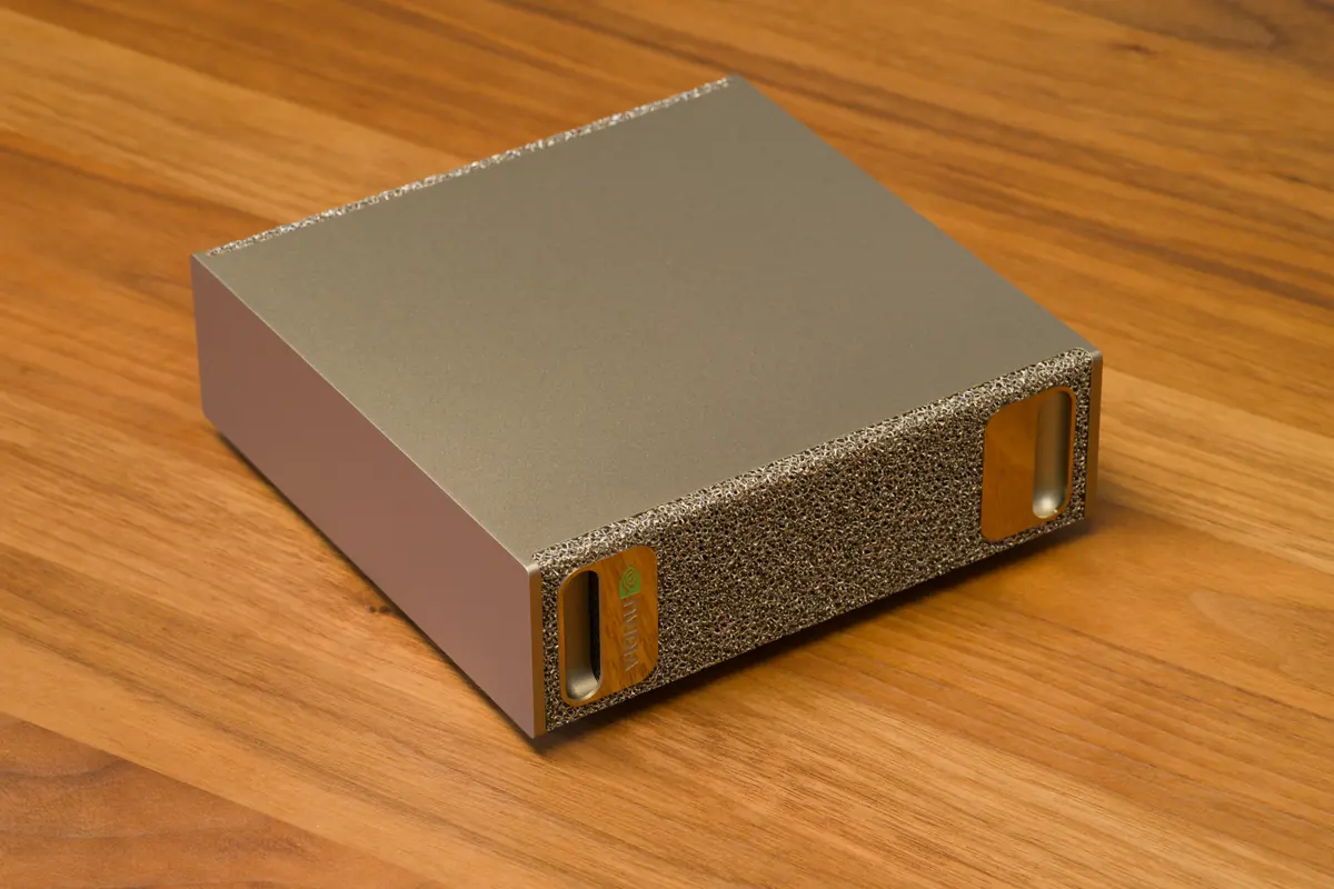
Image credit. Header photo: NVIDIA DGX Spark by Daniel Lu, CC BY-SA 4.0, via Wikimedia Commons.